- Home
- News & Events
- News
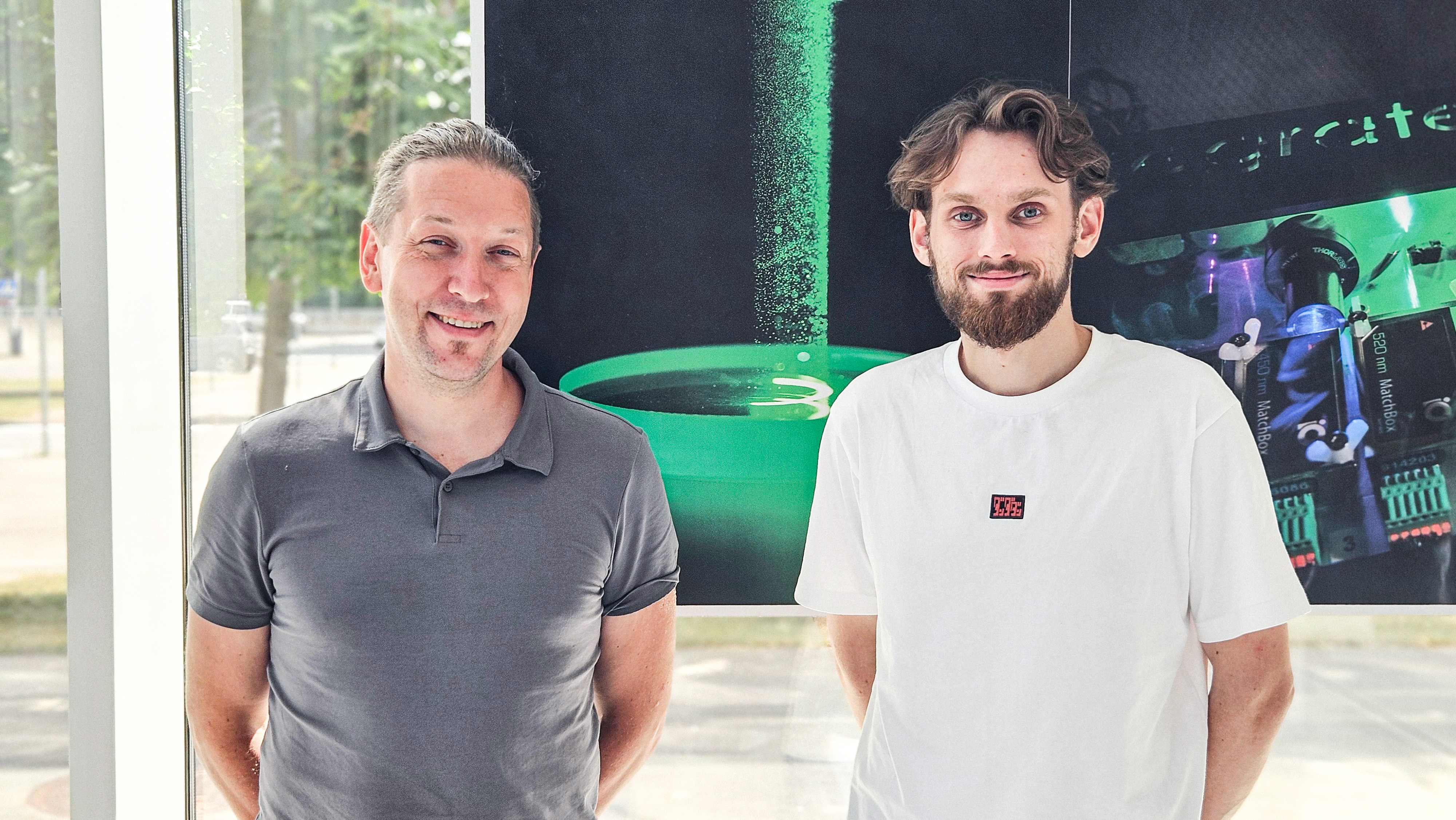
Crystal Defects That Deliver Benefits: FTMC Scientists Contribute to Research Paving the Way for New Quantum Technologies
More powerful computers, safer communications, and increasingly sensitive sensors: a new wave of quantum technologies is approaching. Lithuanian scientists are contributing to the research that is helping drive this progress.
Physics from the Department of Fundamental Research at the FTMC, Dr Lukas Razinkovas and Dr Vytautas Žalandauskas, together with an international team of scientists, have carried out a study whose results were published in the prestigious journal Advanced Functional Materials.
Physicists are investigating so-called "quantum defects" in crystals, atomic-scale imperfections within materials that are invisible to the naked eye. Owing to their remarkable properties, these defects can be exploited in the development of advanced devices, including quantum computers.
Using powerful supercomputers, the FTMC team conducts theoretical calculations in this field. Razinkovas and Žalandauskas developed new methodologies that enable highly accurate predictions of the optical properties of such defects. The research itself was carried out in collaboration with the world-leading Max Planck Institute for Polymer Research.
Defects That Prove Beneficial
When we think about the interior of a crystal, we usually imagine its atoms arranged in highly ordered, periodic patterns. This arrangement extends throughout the material, making the crystal appear identical regardless of where it is examined. However,d crystals are never perfect. They invariably contain a variety of imperfections: an atom may be missing, one atom may be replaced by another, or the regular structure may be disrupted in some other way. These imperfections are what physicists refer to as defects.
“In everyday language, the word ‘defect’ usually implies something undesirable or faulty. In crystal physics, however, defects can be precisely what give a material its most interesting and useful properties. As materials physicist Colin J. Humphreys once remarked: ‘Crystals are like people, it is the defects in them which tend to make them interesting!’” says Dr Razinkovas.
.jpg)
(Crystal structure of silicon carbide containing a silicon-vacancy defect. The diagram shows two possible sites within the crystal lattice where this defect may occur. Picture: FTMC / Advanced Functional Materials)
He explains that not all defects are alike. Some have long been used to control the electrical properties of semiconductors and form the foundation of modern electronics. Others, known as deep defects, act like deep traps in which electrically charged particles, known as charge carriers, can become confined. It is only relatively recently that scientists discovered that certain deep defects possess exceptional optical and quantum properties.
What are these special properties? Some deep defects, also known as colour centres, behave like tiny atomic-scale light sources. When illuminated with laser light, they absorb energy and subsequently emit light of their own. A single defect can emit individual particles of light, known as photons, making them highly attractive for applications in quantum optics and secure quantum communication technologies.
Moreover, some defects behave like miniature quantum magnets. Their quantum states can be controlled using laser light or microwaves and read out with remarkable precision. As a result, such defects can function as extremely small and sensitive sensors for magnetic fields, temperature and other physical quantities, while also serving as quantum bits, or qubits, for quantum information processing. The defects investigated by the Lithuanian researchers exhibit precisely these characteristics: they can act both as single-photon sources and as controllable quantum systems.
“One of the most widely used solid-state materials for quantum technologies is diamond. In it, a carbon atom may be replaced by a nitrogen atom, leaving a neighbouring vacancy in the crystal lattice. This defect is known as a nitrogen-vacancy (NV) centre. It is among the best-studied quantum defects and serves as a benchmark system in the field. Its quantum states can be controlled with high precision, and its potential applications range from quantum sensing to quantum information technologies.
However, diamond also has its limitations. Producing exceptionally pure diamond suitable for quantum technologies is complex and costly, while the processing techniques and device-fabrication technologies associated with diamond are not as mature as those available for conventional semiconductors. Consequently, scientists are searching for alternative materials that can host suitable quantum defects while also being more practical for technological applications,” explains Razinkovas.
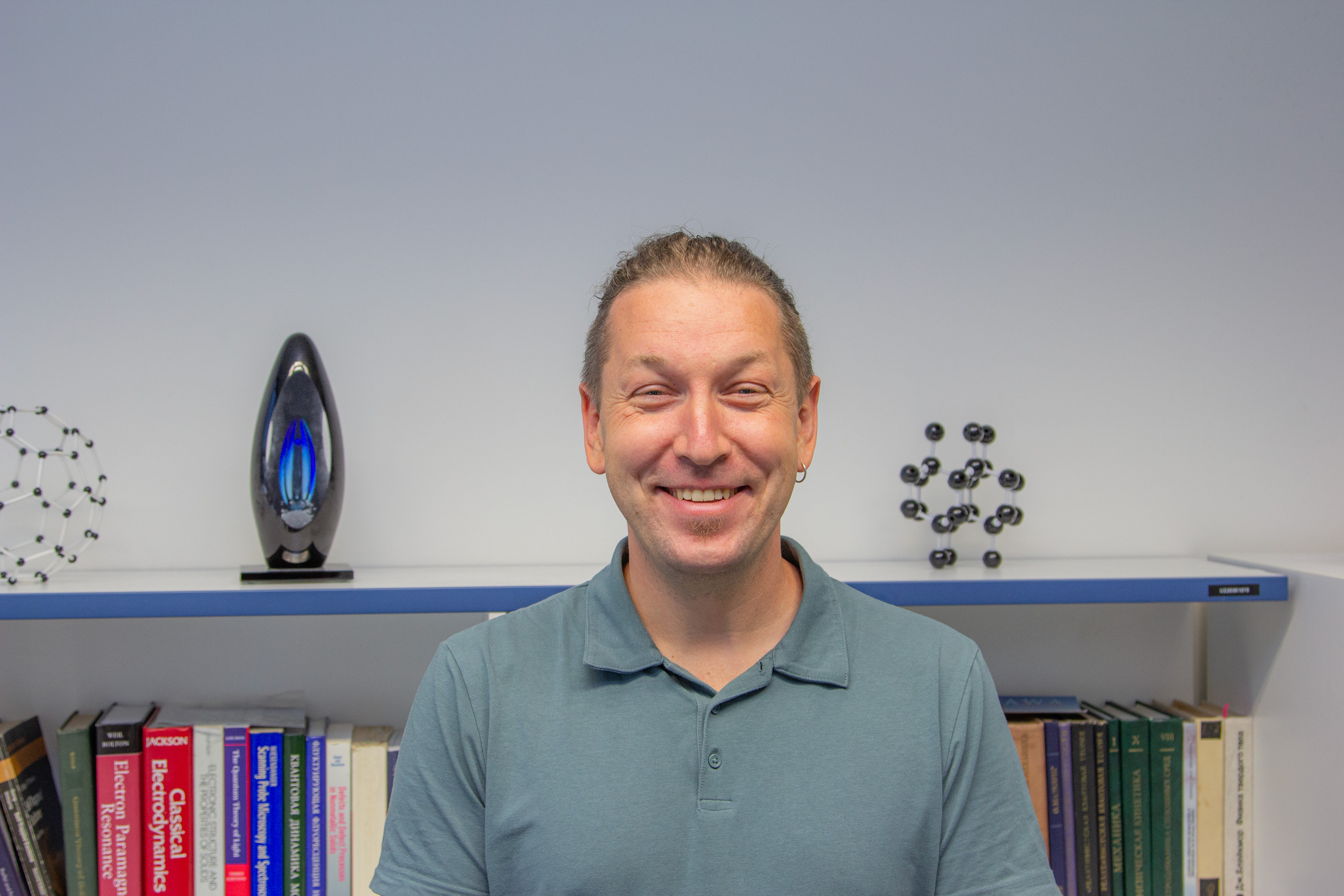
(Dr Lukas Razinkovas. Photo: Gabrielius Mackevičius / FTMC)
Exploring Promising Crystals
According to the researchers, one such alternative to diamond is silicon carbide, a crystal composed of silicon and carbon atoms. This material is already widely used in power electronics for solar energy systems, electric vehicles, communications equipment, and a range of other applications.
“With our international team of researchers, we investigate how defects suitable for quantum technologies behave in silicon carbide. Such research has both an experimental and a theoretical side. On the experimental side, physicists use lasers, magnets and other equipment to perform measurements and observe how these defects ‘behave’.
However, observation alone is not enough. It is equally important to understand why they behave the way they do and to uncover the underlying principles governing their behaviour. This is where theoretical, or fundamental, science becomes essential, and that is precisely the area in which we work. By combining state-of-the-art experimental and theoretical methods, we have uncovered the electronic structure of two important defects,” says Dr Vytautas Žalandauskas.
FTMC researchers investigate theoretically which electronic states form around a quantum defect and how these states interact with vibrations of the crystal lattice. These properties determine how a defect interacts with light, what happens to it after excitation, and which quantum properties it exhibits.
“Until now, the electronic structure of these defects had not been fully understood. We have succeeded in resolving that.
Once you understand what is happening inside a defect, you can begin to identify ways of improving or controlling its properties. Without such knowledge, researchers would be working almost blindly. Measurements reveal outcomes, but they do not always explain their underlying causes. Moreover, not all processes can be measured directly. Sometimes an observed effect is merely the consequence of another, hidden process. Theoretical studies therefore help reveal phenomena that experiments alone cannot uncover, providing a foundation for further research and future applications,” says Razinkovas.
A Lithuanian Team Among the World Leaders
This work stands as a successful example of international collaboration between experts from different scientific disciplines. The lead author of the paper is Dr Ronald Ulbricht of the world-renowned Max Planck Institute for Polymer Research (MPIP). The institute is part of the Germany-based Max Planck Society, a prestigious scientific organisation that has produced dozens of Nobel Prize laureates.
“The experiments employed ultrafast spectroscopy, a technique in which crystals are probed using multiple laser pulses separated by extremely short time intervals. This makes it possible to monitor how the states of a defect system evolve over time. Ulbricht is one of the pioneers in applying ultrafast spectroscopy to the study of crystal defects, and his laboratory is among the very few in the world specifically equipped for this type of research.
Ronald carried out the ultrafast spectroscopy measurements and provided us with the experimental data. Together with researchers from Hungary, Norway and Sweden, we analysed the results, formulated hypotheses about the origin of the observed phenomena and tested them through theoretical calculations.
Importantly, our theoretical work went beyond merely interpreting experimental observations. The proposed hypotheses and computational results were subsequently verified through new experimental measurements. In this way, theory and experiment continually informed one another, ultimately allowing us to build a remarkably clear physical picture.
Vytautas and I work in the field of theoretical spectroscopy and develop methods for modelling spectra that, in my view, are among the most accurate in the world for studying defects and solid-state systems. In this study, our computational results matched the experimental data with extraordinary precision,” explains Razinkovas, adding that the crystals used in the experiments were grown by researchers in Japan.

(Dr Vytautas Žalandauskas. Photo from personal archive)
“By combining the results obtained by all participating groups, we arrived at a very clear and, I would say, compelling picture of the electronic structure of these defects.
Prior to our publication, a considerable number of studies had already been devoted to this topic. However, most remained largely at the level of theoretical speculation. Our findings have revised many previously accepted interpretations because, in this case, theoretical predictions were compared directly with experimental evidence.
The ultrafast spectroscopy experiments revealed phenomena that cannot be observed using conventional techniques, while the theoretical models enabled us to explain and validate these findings,” says Žalandauskas.
By Simonas Bendžius